Company type
Home | Mitglieder |
YES-Yield Engineering Systems, lnc.
Target markets
Industries
Portfolio
Certificates
Contact
3178 Laurelview Court
94568 Fremont , CA
94568 Fremont , CA
Contact Person
About this member
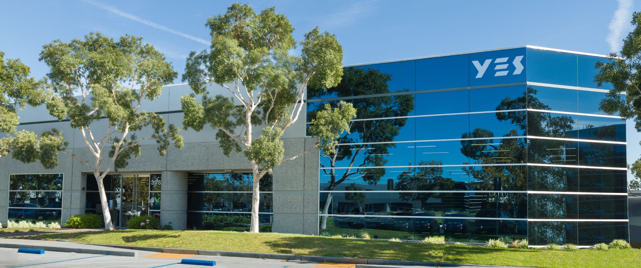
YES Headquarters in Fremont, California
Headquartered in a state-of-the art Silicon Valley facility, with a growing presence in Germany and globally, YES is positioned to be where our customers need us. By delivering scalability, performance, reliability and trust to our partners worldwide, we are committed to enabling them to create the leading-edge products that will drive the next generation of technology breakthroughs – from cellphones and IoT devices, to AI and virtual reality, to diagnostic testing and genetic sequencing – that will power the future.
YES Material Modification and Surface Enhancement Solutions
To create the next wave of technology advances, our customers must transform the materials and surfaces used in their products by implementing novel clean, coat and cure process steps. These transformations not only make new products possible, they also improve manufacturability – allowing engineering breakthroughs to become production realities. YES is committed to developing innovative materials and surface technology solutions that add the greatest value to our customers’ manufacturing processes by lowering their cost, increasing yield and maximizing reliability. We provide a broad portfolio of industry-leading, production-proven solutions to meet these challenges.
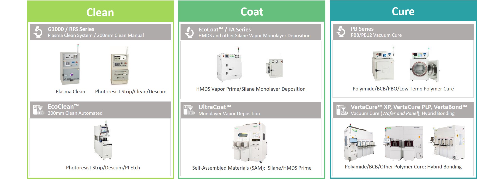
Our Cure systems, which include YES’s flagship Verta- family, use vacuum technology to outgas solvents thoroughly and strengthen bonds, providing superior reliability in just half the time of atmospheric cure. Our Coat systems – the manual EcoCoat and the automated UltraCoat – transform a surface by applying a layer just one molecule thick. This can make the surface hydrophobic such as for microfluidic applications, or adhesive to hold semiconductor photoresist, optical film, or DNA for genetic sequencing. Our Clean technology harnesses the power of plasma to prepare a substrate for processing without damaging sensitive electronics. And our VertaBond system uses vacuum to provide void-free hybrid bonding in reduced time and at lower temperatures.