Company type
Home | Mitglieder |
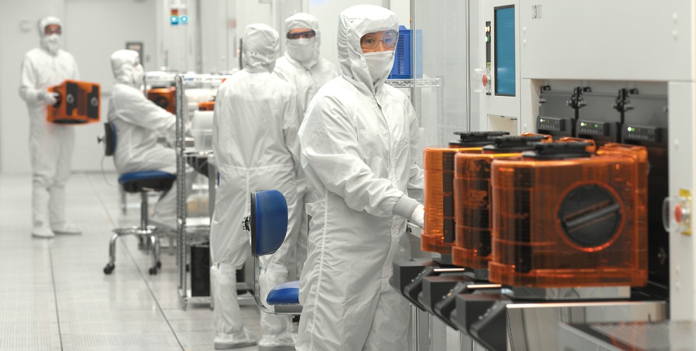
Lam Research GmbH
Target markets
CMP·Etch·Wafer Cleaning
Industries
Micro- / Nanoelektronics
Portfolio
CMP·Computers·Etch·Micro- / Nanoelektronics·Process service·Semiconductor Industry·Wafer Cleaning
Certificates
Contact
Manfred-von-Ardenne-Ring, Haus A 20
01099 Dresden
01099 Dresden
Contact Person
About this member
Von Smartphones und Tablets bis hin zu Wearables und Fahrzeugen - es ist fast unmöglich, dass man mehr als ein paar Stunden verbringt, ohne ein Halbleiter-Funktionselement zu nutzen. Die Halbleiterindustrie berührt fast jeden Menschen auf der Welt und Chiphersteller entwickeln die Technologie weiter, die dies alles vorantreibt.
Als vertrauenswürdiger Partner der weltweit führenden Halbleiterunternehmen nehmen wir Herausforderungen an und bewältigen sie. Aus diesem Grund wird heutzutage fast jeder fortschrittliche Mikrochip mit Lam-Technologie hergestellt. Unsere innovativen Wafer-Fabrikationsanlagen
und Dienstleistungen ermöglichen es den Chipherstellern, noch kleinere und leistungsfähigere Bauteile zu produzieren.
Wir kombinieren überragende Systemtechnik, Spitzentechnologie und eine starke, wertorientierte Kultur mit einem unerschütterlichen Engagement für unseren Kunden.
Products and Services:
Lam Research Corporation has been a major provider of wafer fabrication equipments and services to the world?s semiconductor industry for 25 years and is the market share leader for plasma etch. The Company?s innovative technologies empower customers to build advanced, high-performance integrated circuits.
Throughout its history, Lam has been the technology innovator in the semiconductor etch marketplace. The Company has consistently delivered technology breakthrough that have advanced the state of the art for the semiconductor etch and enabled leading semiconductor manufactures to meet their technology roadmaps goals.
Major breakthroughs include:
- Transformer Coupled Plasma™ technology
- Dual Frequency Confined™ technology
- 2300™ Etch Series with 200/300 mm capability
- Waferless AutoClean™ in situ clean strategy performed after each wafer pass
- Unique technologies that improve the uniformity for today?s most advanced applications
The Company?s focus is on the removal and clean applications area, one of the largest segments of the wafer processing. Customers are many of the world?s leading semiconductor manufacturers, including logic and memory producers, as well as foundries.
Lam’s products selectively remove portions of various films from silicon wafers to create semiconductor devices. The Company?s ValuePoint™ Optimized Productivity Services™ portfolio is designed to optimize customers? equipment sets and support services as needs change throughout their product cycles.
Dielectric Etch:
Based on Lam’s patented Dual Frequency Confined Technology, the 2300 Exelan® family of dielectric etch products addresses challenging technologies node requirements while improving productivity and lowering the cost of ownership for 200 mm and 300 mm wafer processing. The 2300 Exelan Flex™ is the most advanced product in the series.
Conductor Etch:
For 200 mm and 300 mm wafer processing, the 2300 Versys® family of conductor etch products employs a scale version of Lam?s proprietary Transformer Coupled Plasma technology to address leading-edge device structure requirements. The 2300 Versys Kiyo™ for silicon etch is the latest in the series.
Services and Support:
ValuePoint programs offer a portfolio of services and flexible support focused on increasing productivity and reducing total costs. These programs combine Lam?s in-depth expertise and extensive infrastructure to provide customers with the right combination of service, spares, inventory management, and training to meet their specific needs.